

Fab in a Box: A Fully Automated Nanoscale Electronics Manufacturing Platform
Automated Wafer-Scale Additive Printing
At the core of Fab in a Box is a directed-assembly additive printing process capable of fabricating passive and active components directly onto the wafer. Designs are loaded through GDS files, enabling precise translation from concept to nanoscale structures with minimal process overhead. Each layer—interconnects, RF elements, traces, and thermal features—is printed exactly where needed, eliminating the rigid sequencing and retooling demands of traditional semiconductor manufacturing technology. This results in faster development cycles, tighter geometric control, and the ability to support any compatible material system.
Integrated Layer-by-Layer Process Control
Fab in a Box maintains accuracy and repeatability through a fully automated, closed-loop workflow designed for wafer-scale production. Each stage—from wafer preparation to final output—is monitored and controlled for precision, throughput, and alignment. Instead of managing thousands of steps across multiple facilities, teams gain a unified platform that supports rapid iteration and high-volume consistency. This streamlined process sharply reduces complexity and operational overhead compared to legacy semiconductor fabrication workflows.
TECHNOLOGY OVERVIEW
How Fab in a Box Works
Nano OPS created Fab in a Box to deliver fully automated, wafer-scale semiconductor fabrication in a compact, self-contained platform. This system integrates digital design input, additive nanofabrication, and automated process control to build advanced electronic structures with unmatched speed and material flexibility.
20 nm Feature Precision
Our nanoscale printing process achieves feature sizes as small as 20 nm, enabling device structures far beyond the limits of traditional lithography or inkjet-based techniques. This level of nanofabrication precision is essential for next-generation semiconductor devices, flexible displays, and high-performance microsensors. By reducing reliance on subtractive patterning, teams gain more design freedom, tighter geometries, and consistent nanoscale definition across the wafer.

1000x Faster Manufacturing Cycles
The platform prints conductive, semiconducting, and insulating materials up to 1000× faster than inkjet or 3D printing approaches. This acceleration dramatically shortens iteration cycles, allowing engineers to validate and refine device designs at unprecedented speed. By eliminating thousands of steps in the traditional semiconductor workflow, our nanoscale printing method reduces delay, minimizes process bottlenecks, and supports continuous development from concept through pilot production.

PLATFORM CAPABILTIES
What Fab in a Box Enables
Fab in a Box Features
On-demand chips in a few hours
Modular, automated ~10 m² system footprint
No etching, chemical reactions, or vacuum
100 times faster than conventional fabrication
Reduces carbon footprint by more than an order of magnitude
1000 times faster than 3D printing
10-100 times less cost
25 nm to 1000 microns feature size demonstrated

Prototype-to-Production Continuity
Fab in a Box delivers a continuous path from rapid prototyping to scalable manufacturing on the same platform, removing the disconnect that often occurs when designs must transition from R&D tools to full-scale fabs. Teams can prototype new architectures, test and validate structures, and refine designs without retooling or redesigning the process flow. This speeds iteration, reduces development risk, and provides a direct route to reliable, wafer-scale output. The result is a more flexible, responsive approach to semiconductor manufacturing technology that supports faster innovation cycles.
Scalable Semiconductor Fabrication Without a Full Fab
By embedding fab-level capabilities into a compact system, Fab in a Box enables organizations to establish in-house semiconductor fabrication without the cost, infrastructure, or multi-facility requirements of a traditional foundry. Automated precision, additive versatility, and support for complex architectures make it possible to manufacture advanced packaging structures, heterogeneous devices, RF components, and thermal features—all within a clean, efficient workflow. This empowers engineering teams to take control of production, reduce dependency on external fabs, and accelerate product readiness.
.png)

1. Design Input
Electronic device or advanced packaging designs are defined digitally through GDS files and loaded into the Nano OPS system.

2. Wafer Preparation
Wafers are prepared and loaded into the Nano OPS system for processing.
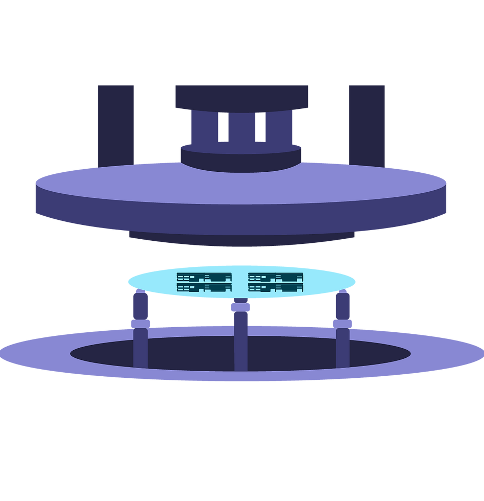
3. Directed-Assembly Additive Printing
Passive and active electronic components are printed directly onto the wafer at the micro- and nanoscale using Nano OPS’ patented additive process.
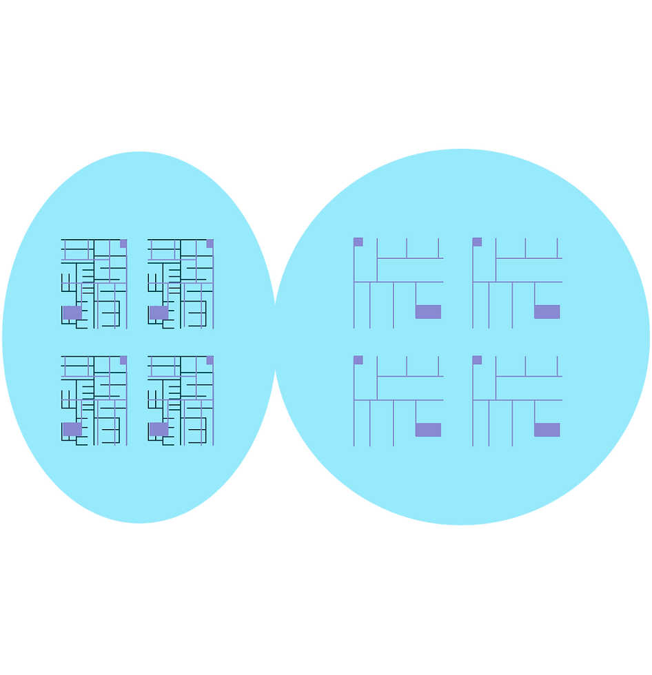
4. Layer-by-Layer Integration
Design changes are implemented quickly without retooling or process redesign.

5. Automated Process Control
The system operates with high precision and throughput through a fully automated workflow designed for repeatability and scalability.

6. Completed Wafer Output
Functional wafers are produced and ready for testing, validation, or downstream integration.