

Microelectronics Applications Enabled by Additive Manufacturing
INDUSTRY APPLICATIONS
Printing of Metal Trace, Interconnects
and Resistors
%E2%80%8B-1.jpeg)
%E2%80%8B-2.jpeg)
%E2%80%8B-3.jpeg)
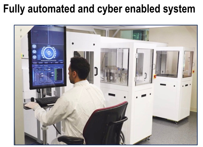
-
Confocal microscope measurements show an average platinum thickness of 250 nm after annealing using RTP at 800 °C for 2 mins
-
The printed Platinum shows uniform and homogeneoussurface morphology.
-


-
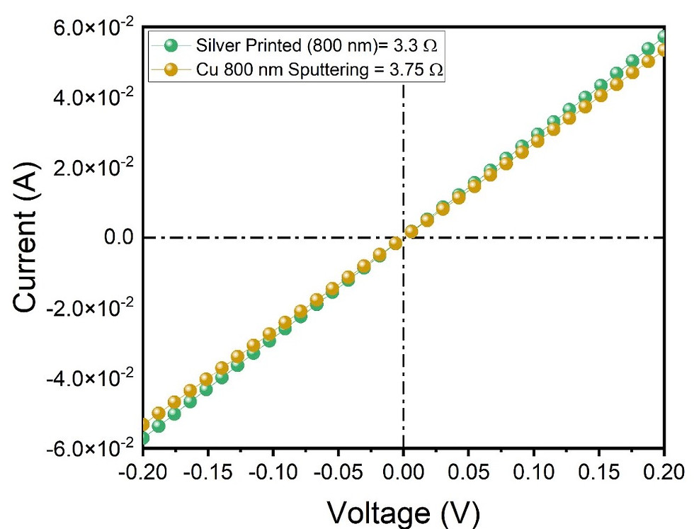
Fan out Flip chip pattern was made using silver
-
The trace’s conductivity is equivalent to sputtered copper at the same thickness.
-


INDUSTRY APPLICATIONS
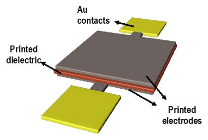
Printing of Dielectric and Passive Components;
Capacitors

-
The SEM images above shows AI₂O₃ micro patterns prepared by directed fluidic assembly with a dielectric constant that matches that obtained by CVD or ALD (𝓔𝒅= 7.2)
-
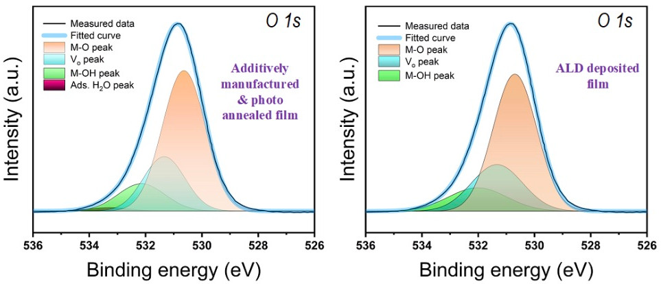
X-ray Photoelectron Spectroscopy (XPS) characterization of the Dielectric Later shows agreement in between ALD and printed films in terns of peak intensities and composition ratios.
-
Higher temperature densification and better dielectric properties for the film.
-
Cross-sectional shows the oxide film thickness variation between 50 °C and 200 °C annealing.
-


-
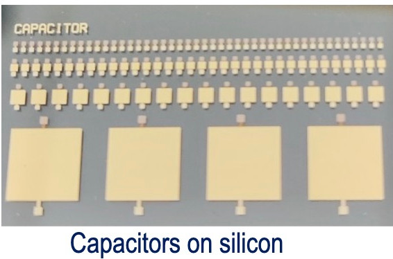
Large-scale fabricated capacitors with a dielectric layer onto sapphire or polymer substrates.
-
Each substrate has 640capacitors with different surface areas of side lengths20, 50, 100, 500, 1000, and5000 µm.
-
Metal: Silver
-
Dielectrics: Al2O3, SiO2, HfO2
-


-
For high-frequency applications, the capacitors need to show reliableperformance under high frequency.
-
The curve shows the capacitance variation versus different frequenciesup to 1 MHz.
-


INDUSTRY APPLICATIONS
Printing of Semiconductors and Active Components; Transistors and Logic Gates
-1.jpeg)
-2.jpeg)
-
Wafer-level manufacturing of 37,000 transistors exhibiting an on/off ratio higher than 106 after annealing.
ACS Applied Electronic Materials, 2023
-
%E2%80%8B-1.jpg)
%E2%80%8B-2.jpg)
-
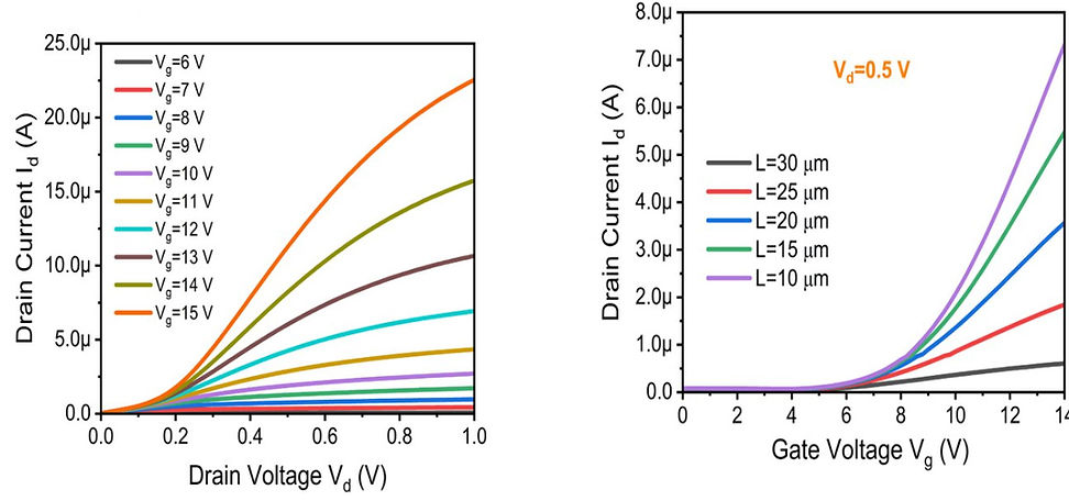
A fully additive liquid-based processprocess to manufacture MOSFETsusing dopants inks to make NMOS.
-
%E2%80%8B-1.jpeg)
%E2%80%8B-2.jpeg)
%E2%80%8B-3.jpeg)
-
A fully additive liquid-based process process to manufacture MOSFETs using dopantsinks. NMOS characterization curves.
-


-
Logic gates such as Inverters, AND, NAND, and NOR were printed
-
The figures below show the fabricated logic circuits (using PMOS)
-
%E2%80%8B-1.jpeg)
%E2%80%8B-3.jpeg)
%E2%80%8B-2.jpeg)
ACS nano, Vol. 18, 2024.
-1.jpeg)
-2.jpeg)
%E2%80%8B-1.jpg)
%E2%80%8B-2.jpg)
%E2%80%8B-1.jpeg)
%E2%80%8B-2.jpeg)
%E2%80%8B-3.jpeg)


%E2%80%8B-3.jpeg)
%E2%80%8B-2.jpeg)
INDUSTRY APPLICATIONS
Advanced Packaging and 3D HeterogeneousIntegration Applications

-
Conventional packaging approaches can notmeet the resolution and density requirements.
-
It can only be done at conventional fabs now
-
Submit DXF or GDS files and load ink, wafers,etc.
-
Additively Manufacture:
-
micro and submicron interconnects.
-
passive components
-
onto silicon, glass or organic substrates (interposers)
-
-


20 nm Feature Precision
Our nanoscale printing process achieves feature sizes as small as 20 nm, enabling device structures far beyond the limits of traditional lithography or inkjet-based techniques. This level of nanofabrication precision is essential for next-generation semiconductor devices, flexible displays, and high-performance microsensors. By reducing reliance on subtractive patterning, teams gain more design freedom, tighter geometries, and consistent nanoscale definition across the wafer.

1000x Faster Manufacturing Cycles
The platform prints conductive, semiconducting, and insulating materials up to 1000× faster than inkjet or 3D printing approaches. This acceleration dramatically shortens iteration cycles, allowing engineers to validate and refine device designs at unprecedented speed. By eliminating thousands of steps in the traditional semiconductor workflow, our nanoscale printing method reduces delay, minimizes process bottlenecks, and supports continuous development from concept through pilot production.

Case Studies
Case studies are available upon request.